LABORATORY OF OPTICS AND ELECTROPHYSICS

Head of the Laboratory -
Dr.Sc. (Phys.-Math.), Professor N.G. Galkin
Staff
Total - 11,
Researchers - 7,
Dr. Sc. - 1,
PhD - 3.
Main research directions
- The development of physical basics of growth technology of new materials based on silicon and buried in silicon lattice nanocrystallites of semiconductor silicides.
- The investigation and modeling of optical, electrical and magnetic properties of low-dimensional materials based on silicon.
- The development and investigation of properties of new types of semiconductor devices on silicon with using of low-dimensional systems.
Principal results
- The processes of epitaxial growth of semiconductor silicide films of Cr, Fe and Mg on silicon, optical and electrical properties of films and its energy band structure parameters have been investigated.
- The processes of conductivity of two-dimensional metal (Cr, Fe, Yb и Mg) films on silicon at the ultrahigh vacuum conditions have been studied.
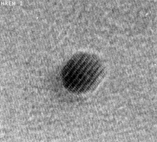
- Multilayer heteroepitaxial silicon structures with buried nanocrystallites of semiconductor silicides of Fe, Cr and Mg have been created and its optical and electrical properties have been studied.
Representative publications
- Galkin N.G., Velitchko T.V., Skripka S.V., Khrustalev A.B. Semiconducting and structural properties of CrSi2 A-type epitaxial films on Si(111).// Thin Solid Films. 1996. V. 280. P.211-220.
- Galkin N.G., Maslov A.M., Talanov A.O. "Electronic structure and modeling of dielectric function of b-FeSi2 epitaxial films on Si(111)" //Solid State Physics, 44 (2002) 688-693.
- Galkin N.G., Goroshko D.L., Dotsenko S.A., and Louchaninov I.V., "Influence of Si(111) 3x 3/30o-Cr surface phase on the formation and conductivity of Fe and Yb monolayers at room temperature" // Thin Solid Films V. 464-465 (2004) 18-22.
- Dotsenko S.A., Galkin N.G., Koval' L.V., Polyarnyi V.O. "In situ differential reflectance spectroscopy study of solid phase epitaxy in Si(111)-Fe and Si(111)-Cr systems" // e-J. Surface Science and Nanotechnology, No 4 (2006) 319-329.