LABORATORY OF TWO-DIMENSIONAL MICROELECTRONICS TECHNOLOGY

Head of the Laboratory -
Dr. Sc. (Phys.-Math. Sciences), Professor A.V. Zotov
Staff
Total- 19,
Researchers - 12,
Dr. Sc. - 3,
PhD - 5.
Main research directions
- Investigation of the formation processes of the ordered nanostructures and low-dimensional structures on semiconductor surfaces.
- Determination of the electrical characteristics and other physical properties of the grown nanostructures.
- Theoretical simulations of the structure and properties of the nanostructures.
Principal results
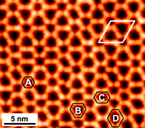
- Using self-assembly processes, ordered arrays of identical-size nanoclusters (magic clusters) were formed.
- Ordered nanostructures built of beryllium-doped silicon nanotubes were formed.
- Effect of structural parameters on conductivity of the surface phases formed by metal adsorbates on silicon was determined.
Representative publications
- Oura K., Lifshits V. G., Saranin A. A., Zotov A. V., Katayama M. Surface Science. An Introduction. Springer-Verlag, Berlin, Heidelberg, New York (2003) 440 p.
- Oura K., Lifshits V. G., Saranin A. A., Zotov A. V., Katayama M. Hydrogen interaction with clean and modified silicon surfaces. Surface Science Reports. 35(1-2), 1-74 (1999).
- Saranin A. A., Zotov A. V., Kotlyar V. G., Kasyanova T. V., Utas O. A., Okado H., Katayama M., Oura K. Ordered arrays of Be-encapsulated Si nanotubes on Si(111) surface. Nano Lett. 4(8), 1469-1473 (2004).